Semiconductor Parts Machining: Tougher Materials, Harder Mass Production
【Introduction】 Semiconductor fabs are expanding, but tougher chamber parts in SiC and ceramics are harder to machine at scale.
Recently, CanSemi, Guangdong's largest wafer fab, went public. Its prospectus shows that Phase 4 of its 12-inch line involves a total investment of about RMB 25.2 billion (≈ US$3.74 billion) and a monthly capacity of 40,000 wafers covering 65 nm to 22 nm, with completion expected by the end of 2029.

When a wafer fab expands, attention usually lands on capacity, process nodes and equipment investment. But behind those numbers lies another thread worth following: the prospectus of Zhenbao Technology, a CanSemi supplier, shows that its direct supplies to CanSemi are chamber components made of silicon, quartz, silicon carbide and alumina ceramics, used in etching and thin-film deposition.
These chamber components were traditionally made of aluminum, stainless steel or ordinary silicon. Today, silicon carbide rings, quartz gas distribution plates, ceramic heaters and alumina structural parts are gradually replacing conventional materials in certain positions.
Upgrading materials solves the problem of whether components can withstand harsh operating conditions. But turning the demand from semiconductor expansion into stable delivery still requires precision manufacturing to answer another question: how do you exploit material performance while ensuring dimensional accuracy, surface integrity and batch-to-batch consistency?
What Actually Changed: Materials That Withstand More
Take CanSemi's production line as an example. A complete chamber involves not one material but several categories — silicon, quartz, silicon carbide and alumina ceramics. They are placed in different positions, replacing or supplementing different components.
CanSemi focuses on power devices and automotive-grade analog ICs, where chamber temperatures often exceed 500°C. Components must resist plasma corrosion, provide insulation and minimize outgassing. Under such harsh conditions, metal parts tend to deform and erode, becoming a source of contamination, while ordinary silicon and quartz also wear faster. That is where tougher silicon carbide and advanced ceramics step in.
Inside an etch chamber, the positions exposed to plasma erosion can be roughly divided into three categories along the chamber space: the focus ring at the wafer edge, the gas distribution plate (also called a showerhead) at the gas inlet, and the large exposed surfaces on the chamber wall and top, such as liners and covers.
All three positions suffer plasma erosion, but each has a different vulnerability — one fears contour change, another fears clogged holes, and another fears failure of large exposed surfaces. The problems that materials must solve differ from the very beginning.
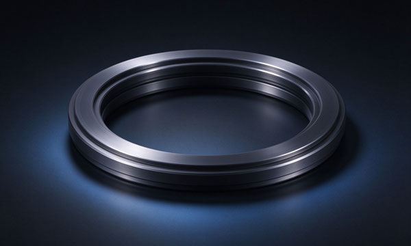
The focus ring sits around the wafer periphery, confining the edge plasma. Its weakness is contour erosion: once the ring's size and shape change, the stability of edge etching is affected.
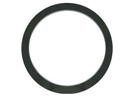
Source: CoorsTek
Focus rings were once commonly made of silicon or quartz. But in some high-power etch chambers, fluorine and chlorine plasma erosion is stronger, so silicon and quartz wear faster and the contour cannot be maintained. Silicon carbide, which resists fluorine-chlorine plasma better, has therefore been pushed forward — the ring erodes more slowly, the contour shifts less, and edge-etch stability gains a little more margin.
The gas distribution plate, by contrast, fears erosion of its holes. To feed process gas evenly into the chamber, it carries a large number of precision holes, so hole diameter, hole position and cleanliness determine whether gas distribution stays uniform. Once holes are eroded or blocked, gas distribution drifts and particles may appear.
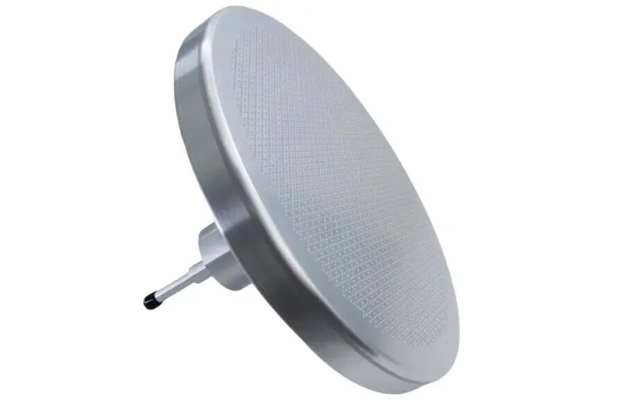
Source: Fortune Precision
But inside some higher-power chambers, quartz wears faster and hole dimensions and wall condition become harder to maintain. Silicon carbide is also replacing quartz in some high-power chambers — it resists erosion better and helps keep hole diameter, position and wall condition stable for longer.
Chamber liners and covers sit on the inner wall and top of the chamber. Their job is to shield the chamber body from plasma, reducing particles and metal contamination caused by erosion of the chamber itself.
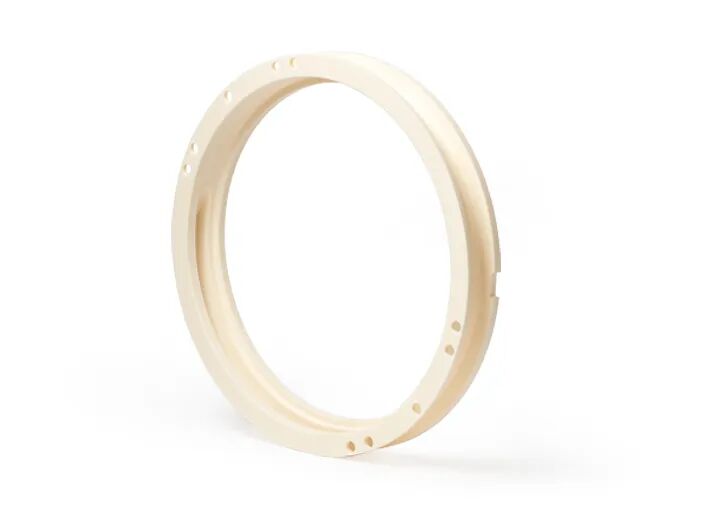
Source: CoorsTek
These positions were once commonly made of aluminum alloy, sometimes with anodizing or coating, and stainless steel and quartz were also options. Aluminum is mature and cost-effective to machine, but under strong plasma its surface erodes; once the coating fails locally, the exposed aluminum substrate can become a source of metal contamination. That is why alumina ceramics — resistant to plasma erosion with outstanding insulation — are becoming increasingly common in these positions.
Tougher Materials — Why Are They Harder to Machine?
CanSemi's expansion sends a market signal: growing AI computing demand is driving wafer fab expansion and higher semiconductor equipment investment.
But expansion is only the surface change. The deeper reason is that AI applications need more computing power, as well as higher bandwidth and larger memory capacity. This is driving the continuous development of advanced logic and advanced memory such as HBM.
As chip structures move toward more complex architectures, the requirements on components keep rising. When some traditional materials or surface-treatment solutions can no longer fully satisfy specific operating conditions, material solutions such as silicon carbide, advanced ceramics, quartz and related coatings attract more attention.
The market is also trending upward. According to QYResearch, the global market for ceramic components used in semiconductor equipment was about US$3.35 billion in 2025, and is expected to reach US$5.50 billion by 2032, a CAGR of about 7.3% from 2026 to 2032.
Market growth means these high-performance material components attract more attention and applications. But moving silicon carbide and advanced ceramic parts from small-batch prototyping to stable volume production usually requires clearing the machining hurdle: low material-removal efficiency, fast tool and abrasive wear, and edge chipping, surface damage and micro-cracks that easily appear during processing.
Take the silicon carbide gas distribution plate in a high-power etch chamber as an example. It carries many precision holes. In prototyping, achieving qualified hole diameter and position on a single part is not difficult. But in batch drilling, tools and abrasives wear fast — after dozens or even hundreds of parts, hole diameters may grow, hole positions may drift, and hole-edge quality declines.
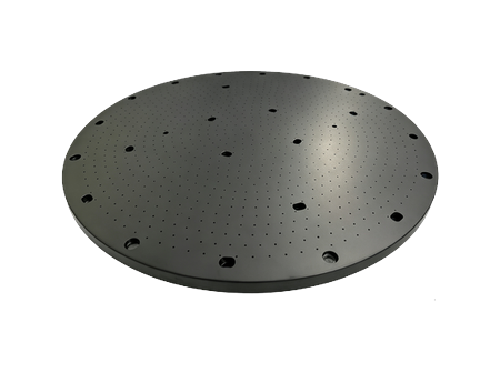
Source: Zhenbao Technology
So the real conflict is not "the more precise, the harder." It is that the more a material withstands the chamber environment, the more machining must answer whether these defects can be kept under control.
Therefore, manufacturing semiconductor equipment components cannot rely on a single material or a single machine tool. It requires combining machining processes, cutting tools, equipment and inspection.
Edge Chipping, Micro-Cracks, Batch Consistency: How the Precision Supply Chain Responds
When components differ in structure, material and precision requirements, machining solutions must be adjusted accordingly.
Precision grinding suits many hard-brittle materials and precision contour machining. Ultrasonic-assisted machining can be used for grinding or drilling of some hard-brittle materials, while in-machine inspection and post-process measurement are used to identify machining errors and verify part quality.
To meet the growing demand for semiconductor miniaturization and integration, Mazak's PALLETECH system uses automated cells of 5-axis machines with turning capability and horizontal machining centers to provide a one-stop solution — covering everything from volume production to high-mix, low-volume production, robot linkage and proprietary system software.
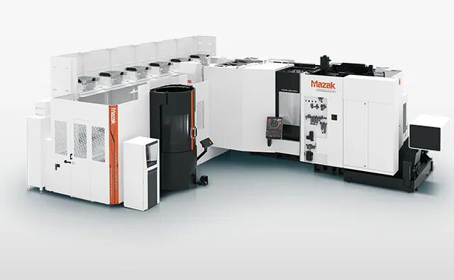
Source: Mazak
For dense-hole, complex-contour parts such as gas distribution plates, Beijing Jingdiao's JDGR500_MG five-axis high-speed grinding center combines five-axis grinding with coordinated process-parameter control to solve micro-cracks and batch stability.
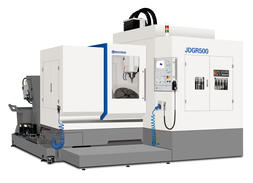
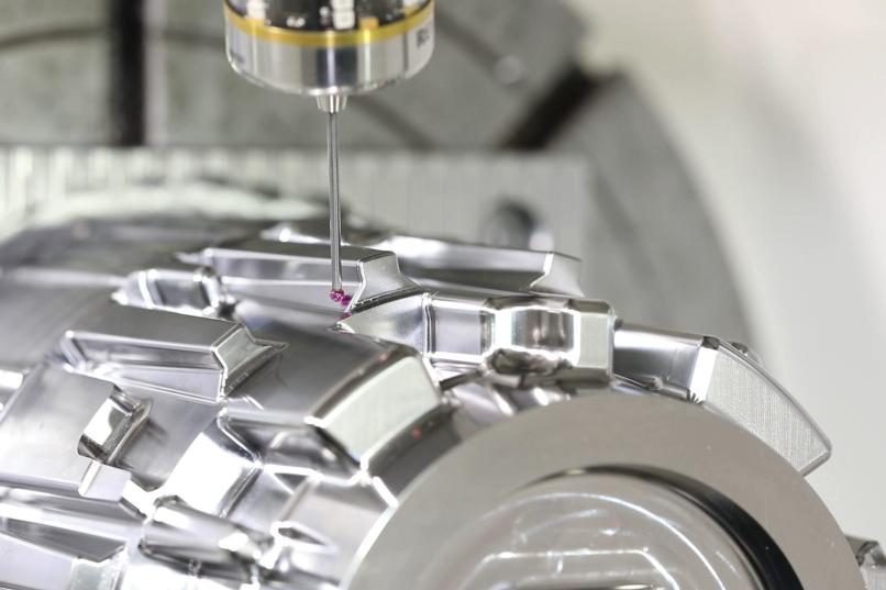
Source: Beijing Jingdiao
For precision grinding of hard-brittle ring parts such as focus rings, Guangdong Kejie Technology's JTGK-600G2 high-speed CNC grinding center is equipped with a high-speed rotary table for multi-mode machining, focusing on contour accuracy and surface-integrity control to solve edge chipping and contour damage.
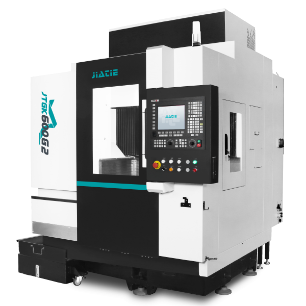
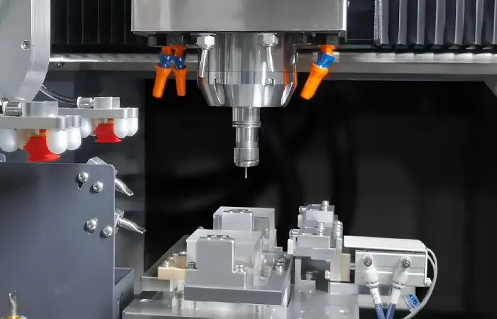
Source: Kejie Technology
For tasks such as hole drilling in gas distribution plates and small-hole machining of hard-brittle components, FANUC's ROBODRILL DC series uses an ultrasonic tool holder to provide a machining solution for edge chipping, micro-crack control and swarf protection in precision drilling.
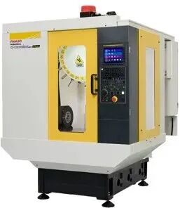
Source: FANUC
For precision machining of ultra-hard-brittle materials, Langen's Ultra 500 ultrasonic precision machining center is equipped with a 32,000 rpm high-speed precision spindle, three-axis linear-motor drive and ultra-high-precision roller guideways to solve edge chipping and hold hole-position accuracy stable at ±0.0015 mm. After machining, quality inspection is still needed. For inspection of such high-precision silicon carbide structural parts, TZTEK's coordinate measuring machine (CMM) with a rotary probe head can perform full-dimension high-precision measurement, ensuring part accuracy meets the strict standards of semiconductor processes.
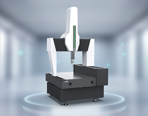
Source: TZTEK
These companies answer the same question with different solutions: faced with specific components, how should precision manufacturers control damage and stabilize batches?
Proven On-Machine Stability and Validation Are What Really Count
For precision manufacturers, the market opportunity is not just in materials and equipment. Moving components from samples to stable supply requires solving a series of problems — material adaptation, process development, surface quality, dimensional consistency and inspection validation.
This link deserves attention for two reasons. On one hand, surging AI computing demand is driving semiconductor industry investment; on the other, fast-growing equipment demand is putting supply pressure on some key equipment. In a market dominated by overseas vendors, this opens a window for local suppliers to enter the supply chain and win more supporting opportunities.
SEMI forecasts that global semiconductor manufacturing equipment sales will reach US$165.9 billion in 2026, up 23.2% year over year. Among them, wafer fab equipment sales are expected to reach US$143.9 billion, up 23.1%.
As AI-related investment keeps growing, the capacity of some overseas equipment makers can no longer fully meet customer demand. The opportunity created by growing semiconductor equipment demand has clearly landed on specific component manufacturing.
For machine tool, inspection, cutting tool and automation equipment companies, the more important market value lies in putting their equipment into the process chain of semiconductor components — from samples to stable supply — so downstream customers can see the core manufacturing capability of the supply chain.
ITES Shenzhen Industrial Exhibition
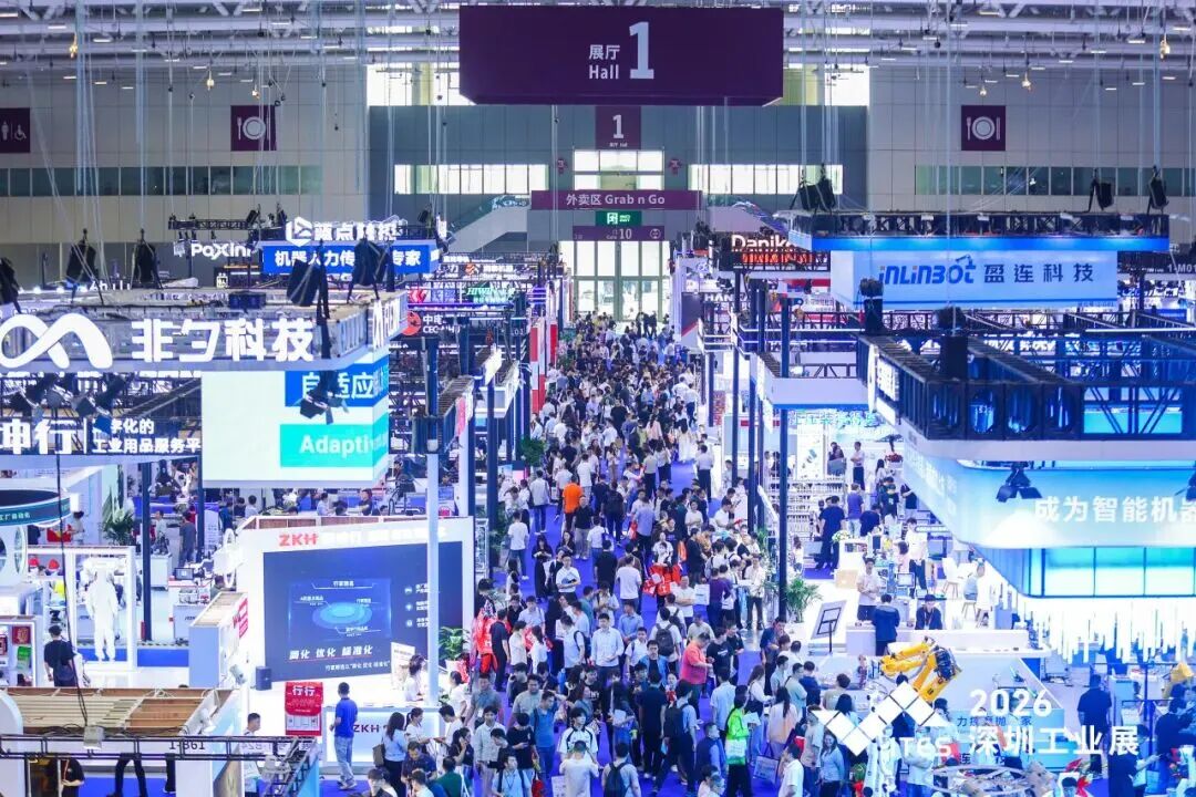
From March 24 to 27, 2027, ITES Shenzhen Industrial Exhibition will be held at the Shenzhen World Exhibition & Convention Center (Bao'an).
On-site buyers come not only from semiconductor equipment and precision component companies, with a focus on chambers, showerheads, valves and ceramic parts in precision grinding, hard-brittle machining, non-destructive testing and batch consistency; BYD, Huawei, CSOT, SiCarrier and other companies will attend in groups with their supporting needs.