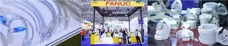
ITES China Shenzhen International Industrial Manufacturing Technology and Equipment Exhibition
Breaking Through Semiconductor Cavity Machining Challenges: How Electrical Discharge Machining Became the Unsung Hero
【Introduction】 Semiconductor cavity、Electrical machining
Introduction: When discussing chip autonomy, we often fixate on lithography machines yet overlook every “hidden bottleneck”: the core mechanical components that run through all equipment, from etching machines to packaging systems. Their machining capability directly determines the performance ceiling of semiconductor equipment. In the precision structures of semiconductor equipment cavities, components like liners, gas distributors, and stator cooling jackets are most typical. They serve critical functions—fluid transfer, precision positioning, vacuum sealing, and thermal management—and a 0.1-micron improvement in their machining accuracy can boost chip yield by approximately 5%.
Among these, vacuum cavities demand absolute sealing and vacuum integrity, imposing stringent requirements on surface finish and high precision. Meanwhile, to withstand extreme process environments, these parts often use materials like alumina ceramics and stainless steel, which are not only hard and brittle but also have extremely dense microstructures.

For this reason, compared to traditional mechanical machining (where tools wear easily), non-contact electrical discharge machining (EDM) stands out by avoiding mechanical stress during ultra-precision machining. But what makes EDM so appealing? And what results does it deliver for machining specialized materials?
01 | The “Precision Fortress” of Cavities: Lies in Structural Components?
As the core reaction chamber of etching and thin-film deposition equipment, semiconductor cavities are not just physical spaces that create and maintain ultra-high vacuum, ultra-clean, and specific plasma environments—they are precision platforms that hold wafers and enable complex chemical-physical reactions.

A typical semiconductor cavity, by function, includes transfer chambers, load-lock chambers, and reaction chambers, primarily made of high-purity, corrosion-resistant stainless steel and aluminum alloys. Compared to transfer chambers, the latter two have higher machining requirements.
Load-lock chambers, mainly stainless steel, connect to different reaction chambers and require tailored surface treatments to ensure cleanliness and corrosion resistance. Reaction chambers, where wafers are processed, host chemical reactions of multiple process gases, demanding exceptional cleanliness and corrosion resistance.

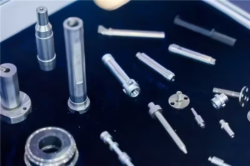
Inside reaction chambers, components are categorized by material and function into metal process parts, metal structural parts, and non-metallic mechanical parts—including gas distributors, trays, cast steel platforms, flow meter bases, cooling plates, and electrostatic chucks. Each part has unique machining requirements that directly impact wafer etch or deposition yield.

For example, electrostatic chucks, the “fixed grippers” during wafer processing, use high-purity aluminum nitride (AlN) ceramic material and electrostatic adsorption to precisely position wafers. Their flatness (error ≤±0.5μm) and adsorption force determine processing accuracy, while the electrode layer and adsorption layer require nanoscale bonding, with coaxiality error of electrode columns controlled to <±0.1μm.

Cavity liners, the “protective barriers” of cavities, directly contact reactive gases and plasma. They must exhibit strong corrosion resistance, wear resistance, and cleanliness to prevent contaminants from entering the processing environment and compromising wafer surface quality. Key specs include: internal flow channel surface roughness Ra <0.1μm; coaxiality of wafer transfer ports and external interfaces at ±0.002mm to prevent gas leakage.

Cooling plates, critical for temperature regulation, use precise flow channel designs for uniform heat dissipation, keeping cavity temperature fluctuations within a micron-level range to avoid impacting wafer processing accuracy. Materials must have high thermal conductivity, with channel surface roughness Ra <0.05μm.
Additionally, complex sealing grooves and interfaces—“connecting hubs” between cavities and external equipment—handle gas transfer and signal conduction. Groove dimensional accuracy and surface roughness directly affect sealing performance and transfer efficiency, requiring depth tolerance of ±0.5μm and sidewall angle error ≤±0.5° to avoid damage from plasma bombardment.
02 | Why Is Electrical Discharge Machining Indispensable?
Machining the above components requires withstanding extreme temperatures, plasma corrosion, and mechanical stress, with geometric accuracy, surface finish, and material purity reaching nanometer or even sub-nanometer levels—standards traditional machining can no longer meet.
Traditional tools, when mechanically cutting hard materials, suffer rapid wear and cause workpiece edge chipping or cracking, severely limiting production efficiency. Some structural parts also require extreme cleanliness, with no burrs or micro-cracks allowed during machining, as these defects would compromise the vacuum environment and wafer quality. EDM machines, operating on the principle of “material removal via pulsed electrical discharges,” break free from the dependence on tool hardness and cutting force in traditional machining. They offer unique advantages in precision control, material adaptability, and efficiency.

The core lies in their non-contact method: electrodes and workpieces do not touch directly. Instead, high temperatures from pulsed discharges erode material, avoiding workpiece deformation caused by mechanical cutting forces. Moreover, EDM machines boast exceptional dimensional consistency, with batch-produced cavity components having dimensional deviations controlled within ±0.001mm, drastically reducing assembly errors in semiconductor equipment.
As new materials proliferate, component sizes grow more extreme, and requirements for machining complexity, fineness, and precision rise, demand for EDM technology will continue to surge.
03 | Global Top-Tier Solutions Gather: A Technological Race Among Brand Manufacturers
Responding to the urgent demand for EDM in the semiconductor industry, global leading manufacturers have rolled out tailored solutions to empower precision manufacturing.
In terms of material adaptability, UNITED MACHINING’s FORM P600 integrates an Intelligent High-Speed Pulse Power Supply (ISPG) and iGap technology to optimize each discharge, improve discharge distribution, maximize material removal rate, and maintain high-precision surface quality—solving the pain point of “hard materials being difficult to machine.”
For high-end semiconductor cavity components, its AgieCharmilles CUT P 350 Pro wire-cut EDM machine features “adaptive pulse technology” to adjust discharge parameters in real time based on workpiece thickness. Its Automatic Slug Welding (ASW) function reduces manual intervention and frees up machining time, making it ideal for core cavity parts like precision flow channels.

Sodick’s AQ1200L wire-cut EDM machine uses linear motors, linear gratings, and a mechatronic structure for superior positioning accuracy, minimal setup space, and a large machining area. Its AL60G+ machine now supports copper graphite (CuCr) machining of superhard alloys, suitable for mass-produced semiconductor parts like lead frames and heat dissipation cavities in packaging equipment. Equipped with AI-powered machining and a 3D EDM CAM system, it automatically optimizes discharge parameters to cut labor costs.

Makino focuses on multi-dimensional machining of complex cavity components. Its EDAC series can machine minimum R-angle radii of just 5μm, with excellent surface roughness as low as 1.3 μin Ra (0.25 μm Rz), delivering high accuracy and surface processing capabilities. For heterogeneous material machining, Makino’s hybrid machining centers enable integrated metal-ceramic processing. The EDAF2i Ultra machine adds process data support for domestic materials, excelling at meeting semiconductor manufacturing’s stringent requirements.

Beyond these general advantages, EDM plays a key role in addressing new industry trends—large-size and ultra-thick machining. In advanced packaging, for instance, growing mold sizes pose extreme challenges for wire-cut machining of ultra-thick workpieces over 1000mm. The industry is now tackling issues like stable fluid supply and efficient chip removal under high-energy discharge to boost efficiency and surface quality—this is the cutting-edge direction of EDM innovation.
At next year’s ITES Shenzhen Industrial Exhibition, these companies will showcase their latest industry solutions and equipment. Additionally, leading firms like Yamazaki Mazak, Tsugami, Yasda, Rhodes, FANUC, Mitsubishi Electric, Genius, Beijing Jingdiao, Kejie Technology, Gree Intelligence, Shuofang, Lijin, Takisawa (Nidec), Oto (TAJMAC-ZPS), Evermi, and Jieyongda are also gearing up. Stay tuned!
ITES Thematic Exhibition - Metal Cutting Machine Tool Show’s EDM Machine Zone: Targeting mold manufacturing, 3C electronics, auto parts, aerospace, and medical devices, this zone showcases wire-cut EDM machines, sinker EDM machines, and more. Leveraging instantaneous high-temperature material removal via high-frequency pulsed discharges, it machines high-hardness conductive materials (e.g., cemented carbide, titanium alloys) to micron-level accuracy. (Click “Read More” at the end for exhibition details.)
If you are interested in the semiconductor industry chain, have innovative machining solutions, and wish to engage with leading enterprises like CSOT, Osram Opto Semiconductors, BYD Semiconductor, Kanghui Semiconductor, AMEC, and Changyuan Technology to explore partnerships, scan the QR code to contact us. Secure your spot at the 2026 ITES Shenzhen Industrial Exhibition and book prime exhibition spaces now!