ITES China Shenzhen International Industrial Manufacturing Technology and Equipment Exhibition
A Single Mold Powers a Billion-Dollar Market: Where Lie the Challenges in Precision Development of Lead Frames?
【Introduction】 IC Manufacturing (Wafer Fabrication, Packaging & Testing Technologies & Products)、3C Electronics、Mold Manufacturing
Lead: Behind a semiconductor lead frame, precision molds are quietly exerting their influence?
As the electronics industry continues to expand, the global lead frame market reached RMB 27.92 billion in 2023 and is projected to exceed RMB 35.2 billion by 2029, with a steady compound annual growth rate (CAGR) of 3.8% from 2023 to 2029. A sub-sector with a scale approaching RMB 100 billion is accelerating its formation.
In terms of market structure, the global lead frame industry exhibits a "leader-concentrated" pattern. The top eight enterprises, including Toshiba Tec (Japan), Changhua Technology (Taiwan, China), and Shin-Etsu Electric (Japan), collectively control approximately 60% of the global market share. Domestically, the Yangtze River Delta and Pearl River Delta regions serve as core production bases. Enterprises such as Kangqiang Electronics and Sanjin Electronics are driving accelerated domestic substitution of lead frames through technological breakthroughs.
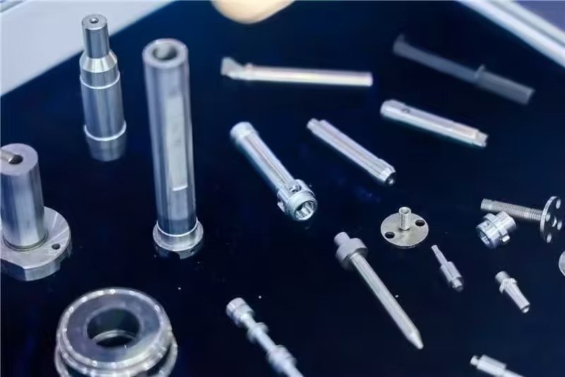
However, in the process of transforming a metal strip into a "bridge for chips," why are micro-meter precision molds both the "yardstick" determining product accuracy and the "critical lock" constraining production capacity?

The Three Roles of Semiconductor Lead Frames
A semiconductor lead frame is a critical structural and functional component in semiconductor packaging, typically made from metal materials (e.g., copper alloys, iron-nickel alloys) via stamping or etching processes. Thus, it can be categorized into stamped lead frames and etched lead frames. Stamped lead frames, leveraging cost and efficiency advantages, dominate the market, accounting for approximately 74% of the total.

In chip packaging, lead frames perform three key roles:
1. Mechanical Support: They bear chiplets-sized chips, maintaining the overall stability of the package structure and preventing chip damage during subsequent assembly and use.
2. Electrical Connection: Through bonding materials (e.g., gold wires, copper wires), they connect the chip’s internal circuits to external leads, enabling efficient and reliable electrical signal transmission.
3. Heat Dissipation: They rapidly conduct heat generated by chip operation to external cooling structures, preventing high temperatures from impairing chip performance and lifespan.

In traditional packaging, without high-precision lead frames, even high-performance chips would struggle to be practically applied—precisely where mold manufacturing precision dictates lead frame accuracy.
As the "Lifeline of Precision," What Makes Molds So Challenging?
Currently, mainstream lead frames rely on stamping processes, involving stages such as precision mold fabrication, high-speed strip stamping, high-speed selective electroplating, plating die production, cutting and leveling, cleaning and testing, and packaging.

Take common SOP-series lead frames, for example. Production requires multi-station progressive dies for high-speed stamping: over 500 strokes per minute, with lead spacing typically less than 0.5mm, and micro-meter dimensional precision (e.g., wire-cut cavity precision must be controlled within ±2μm). This process demands synchronized debugging of press parameters and stamping force control—complex operations that further impose stringent requirements on mold geometric precision and surface roughness.
As chip nodes advance, lead frames are evolving toward miniaturization and higher precision. Beyond "micro-meter precision," stamping molds face three technical challenges:
1. Withstanding High Impact While Maintaining Durability:
High-precision molds must endure high-frequency impacts of thousands of strokes per minute while ensuring a service life exceeding tens of millions of strokes. This necessitates materials like SKD11 or cemented carbide, with surface treatments such as carburizing and PVD coating (e.g., TiN) to extend punch life—ordinary steel cannot meet these demands.
2. Achieving High Precision with Minimal Tolerance:
Stamping pitch precision must remain within 0.02mm, with cumulative error not exceeding 0.05mm, and blanking burrs less than 0.02mm. Die blade precision and clearance control must be accurate to within 0.01mm; otherwise, lead deformation, short circuits, or poor soldering may occur. Traditional processing techniques struggle to achieve this. For molds with "T"-type, "M"-type, or other irregular cross-sections and high-density lead designs, the precision requirement for punch and die reaches 2-3μm, making processing extremely difficult.
3. Maintaining Conductivity While Resisting Deformation:
Lead frames often use high-conductivity copper strips, requiring over 90% conductivity and sufficient Vickers hardness. During stamping, molds must avoid material fracture while preventing deformation—an extremely demanding balance of stamping force and angle control.
Who Can Address the Challenges in Precision Mold Manufacturing?
What cutting-edge processing solutions are currently being developed to tackle long-standing pain points in mold manufacturing?
Precision molds depend on precision machine tools. For instance, Huaying Guangbao produces lead frame molds requiring cavity processing precision of ±2μm, surface roughness Ra 0.05μm, and cumulative error of cavity alignment across a 500mm-long template controlled within 0.005mm. To achieve this, the company uses Makino’s high-precision oil-based wire-cutting machine tools, capable of 0.05mm minimum wire diameter cutting, paired with optical curve grinding for shaped punches—perfectly matching mold precision requirements.
Similarly, Mazak’s UD-400/5X 5-axis machining center, featuring a gantry structure and a 45,000 RPM electric spindle, enables high-precision cavity processing (±2μm). Yasda’s YMC650 machining center achieves ISO230-2 positioning precision of 0.0006mm and repeat precision of 0.0002mm—both serve as "core equipment" for high-end mold manufacturing, meeting the needs of semiconductor lead frame mold production. Notably, these leading enterprises will gather at Booth 7, ITES Shenzhen Industrial Fair next March, with original manufacturers presenting solutions tailored for semiconductor component processing.

Beyond mold manufacturing, suppliers across the industrial chain are actively advancing technological innovations to enhance quality and efficiency in lead frame production.
-From Encapsulation Materials:
Boway Alloy has achieved domestic substitution in semiconductor lead frame materials (e.g., C18150, C7025 alloys), breaking foreign monopolies.
Jinchuan Group’s integrated forging production line for high-end special-shaped copper strips, paired with self-developed 1,250kN high-frequency heavy-duty forging equipment, enables precise forging at 1,000 strokes per minute. This balances 0.015mm stamping precision with the dual requirements of copper strip "high conductivity + high hardness."
-From Technological Innovation:
Kangqiang Electronics has broken through 2μm ultra-fine pitch technology, ranking first domestically in etched lead frame market share. In 2025, it will launch third-generation EMC epoxy molding compounds, compatible with Chiplet advanced packaging.
Huatian Technology has developed dual-ring QFN lead frame technology, overcoming limitations of traditional single-ring lead layouts. By arranging leads in inner and outer rings, it significantly increases lead count and optimizes signal transmission performance.
If you are interested in the semiconductor industry chain, have innovative processing solutions, and seek to connect with leading enterprises such as CSOT, Osram Opto Semiconductors, BYD Semiconductor, Kanghui Semiconductor, SMIC, and Changyuan Technology to explore collaboration opportunities, secure your golden booth at ITES Shenzhen Industrial Fair 2026 now.
.jpg)
Every small step forward in components—from lead frames to precision molds—represents a giant leap upward for China’s semiconductor industry. The pace of domestic substitution in high-end lead frames may accelerate faster than we imagine.